custom mechanical keyboard
Electronics - hardware
Schematic
I used an Atmega32u4 microcontroller because it has a built-in USB interface that comes with a pre-configured bootloader. Therefore I could program and give power to the device solely through USB. Breaking out the ICSP pins or implementing a USB to UART IC into the design was not necessary.
This portion of the schematic is mainly interfacing the Atmega32u4 so it can successfully operate. This requires an external crystal, bypassing with 0.1uF capacitors on each power pin, and a 10uF capacitor on the VBus line. Pin 33 (PE2) is tied to ground so on reset the microcontroller always executes the bootloader. The rest of the schematic is wiring of the reset switch and the USB according to their datasheets.
The matrix was wired in the schematic so it resembled the physical layout of the keyboard. This helped with programming syntax down the line. This matrix also allowed the microcontroller to read the inputs of 52 switches by only using 19 I/O pins.
In the program, the columns are set as outputs. The rows are set as inputs and tied to ground with internal pull-down resistors in the microcontroller. This prevents a floating input. To read a key, the microcontroller sets one column high and the rest low. Rows in that corresponding column are then read to see if any are pulled high. If it is, then a switch has been pressed. For example, if Column 1 is set high and S1 is closed, Column 1 will now be electrically connected to Row 1. The microcontroller will read Row 1 as high, and interpret this as a key press from S1. All of the columns are scanned using this process to detect a key press across the entire keyboard (Column 2 is then set high and the rest are set low, Column 3 is then set high and the rest are set low, etc). But what if I press a switch in Column 4 when the microcontroller is setting Column 1 high? Will there be trouble reading this switch since Column 4 is set low when I’m currently pressing the switch? This scanning process happens so quickly that this doesn’t matter. The microcontroller will eventually set Column 4 high before you even have time to physically release the switch, so the press will still be detected.
Diodes are used on every switch to prevent ghosting. Ghosting is when a key press is detected when its corresponding switch hasn’t been pressed. For example, let’s say that no diodes are present in the circuit and S1, S2, and S17 are pressed at the same time. If Column 1 is set high, current will flow through S1 into Row 1. However since S2 and S17 are also closed, the current will flow from Row 1 through S2, then down Column 2 and through S17, and eventually to Row 2. Therefore, the microcontroller will read Row 1 and Row 2 as high. So when Column 1 is high, Rows 1 and 2 will also be high and the microcontroller will interpret S16 as closed and output a Tab even though the physical key hasn’t been pressed. Diodes prevent the current from flowing this way, thus getting rid of ghosting.
PCB Layout
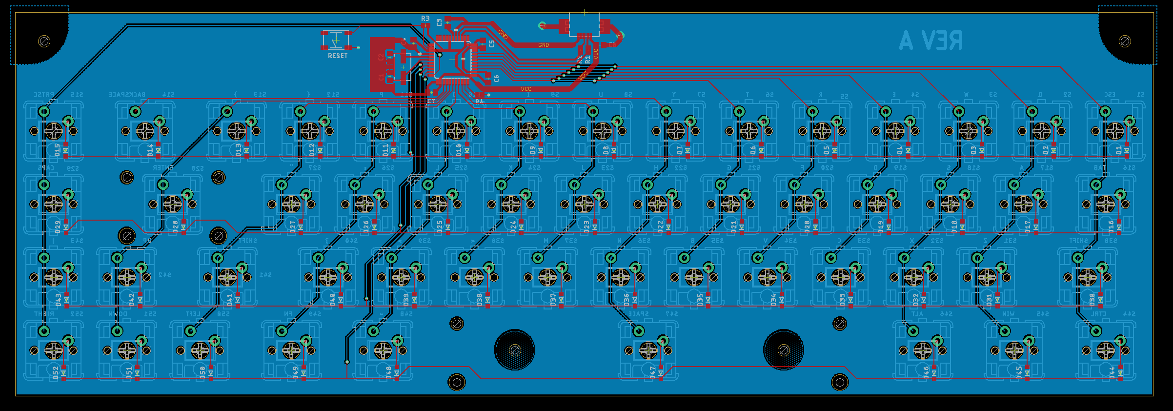
I used a two layer board to layout the PCB. Most of the traces were routed on the top layer while the bottom layer was used for any left over traces and a ground plane. The switches were placed on the PCB first because their position was governed by their key size. A 1U key had to be 1U (19.05mm) away from its adjacent switches, a 1.25U key had to be 1.25U away from its adjacent switches, etc. I wanted the USB to be placed in the middle of the board, so its location was also fixed and placed onto the PCB next.
The rest of the routing was pretty standard. The remaining components were placed on the PCB to make the traces short (especially those from the USB to the microcontroller, the bypass capacitors to the microcontroller, the crystal to the microcontroller, and the 10uF capacitor on the Vbus line to the USB). A localized ground pour was placed around the crystal and its two capacitors then tied to the main ground line through a single via to reduce interference. Four M3 mounting holes were also made so the PCB could be attached to an enclosure.
Manufactured PCB
Soldering the PCB
I drag soldered the microcontroller and USB header pins. For the other SMD components I first tinned one pad then placed the component on its footprint. Once placed, I heated the tinned pad until a connection was made with one side of the component. Afterwards, I soldered the other side like normal.
firmware
Current Firmware: https://github.com/ress059/Mechanical-Keyboard
making the keycaps
A keycap design that was optimized for FDM on my personal Ender 3 printer was created in Solidworks. 3D printing allowed me to create custom text that was not readily available on keycaps sold online. There were also fewer geometric constraints I had to follow compared to other manufacturing methods.
The keycaps were made to fit CherryMx style switches. Separate STL files for the text and keycap body were created so I could change the filament color after the text was printed. In the keycap models, 0.16mm text was debossed into the top surfaces. I then set the z-hop in my slicer to 0.2mm. This made the nozzle move up by 0.2mm whenever it traveled across the debossed section of the keycap. Therefore, the nozzle would never hit the text that was printed in the previous step. The initial layer height for the keycap was set to 0.16mm, the same height as the text. Therefore, there would be no interference when printing the 2nd layer of the keycaps.
The rest of the keycap was then printed like a normal model. The remaining layers were printed at a height of 0.08mm which produced a really nice result. In my slicer, I also enabled retraction and tweeked the settings to minimize stringing, but some was unavoidable. I just manually removed any stringings afterwards.
making the enclosure
CAD Design
CAD models of individual parts and the assembly were first created. A 3D model of the PCB was used to properly dimension the mounting holes, USB opening, height, and shell of the enclosure. The rest of the design was focused on a balance between durability and aesthetics. The CAD models below show the final design and how the keyboard is fully assembled.
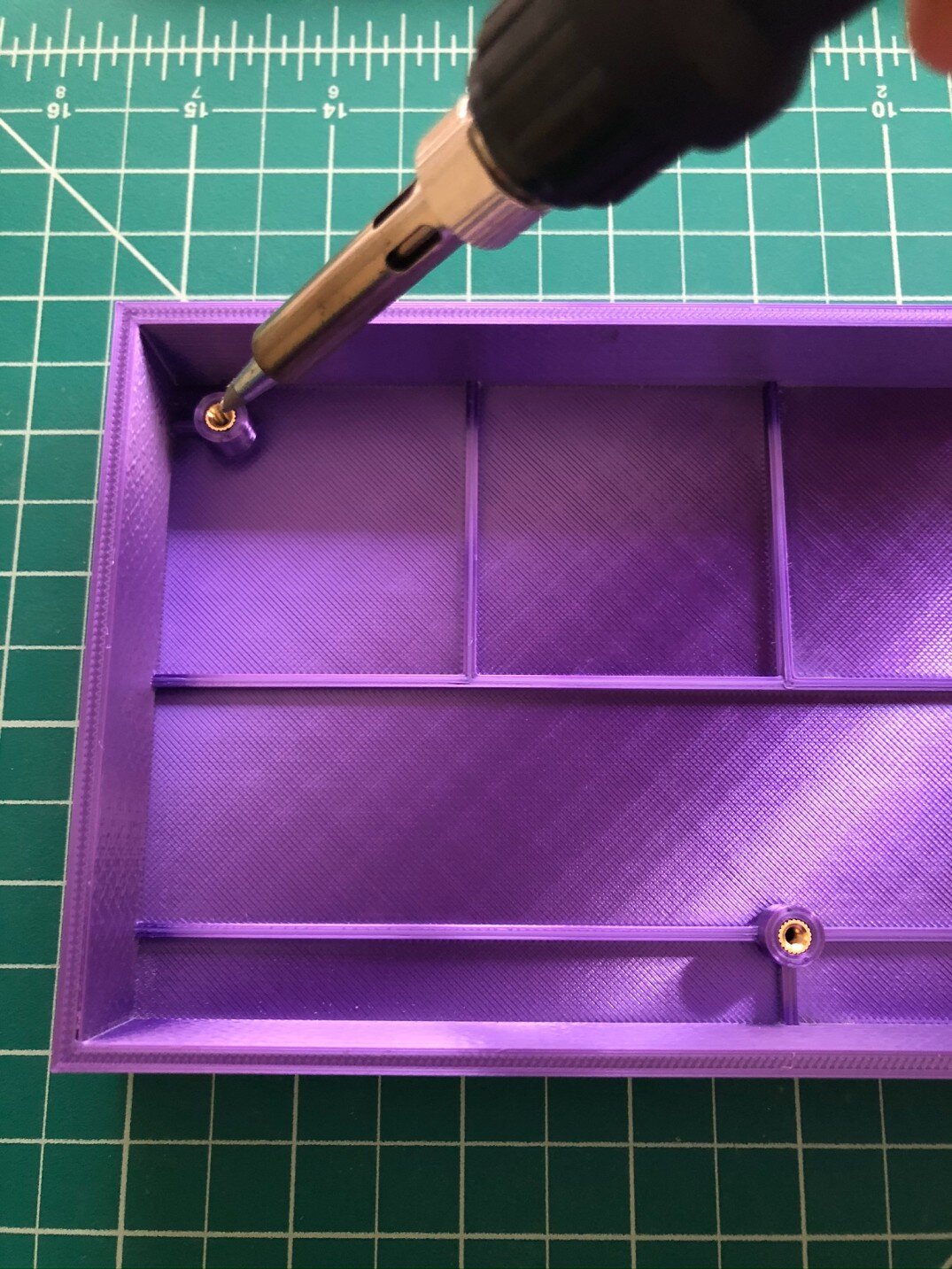
M3 brass inserts are first thermally inserted into the mounting holes of the bottom piece of the enclosure.
Afterwards, M6 x 0.5 x 6 screws and M3 washers are used to secure the PCB to the two lower mounting holes of the bottom piece. The keycaps are then snapped onto the switches.
A separate piece is then used to cover up the rest of the PCB and the upper portion of the USB port. M3 x 0.5 x 20 screws and M3 washers are used to secure the top piece and the rest of the PCB to the bottom piece.
No fillets were used for the same reasons as the FDM keycaps. I was not worried about any stress concentrations that may occur in the corners because a keyboard is a relatively low force application. This also increases printing accuracy because the X and Y stepper motors can be used separately whereas a fillet needs motion from both of these motors simultaneously. Ribs were used to reinforce the mounting holes and bottom shell. The thickness of the shell was limited by the USB port. Too large of a thickness would not allow the cable to be properly inserted. Therefore, a shell of 3.6mm was used. It was thick enough to be durable while thin enough to look good and give proper clearance for the USB. This was also divisible by the nozzle diameter of 0.4mm so a wall with no gaps could be printed.
Bottom Artwork Design
Once the enclosure was fully modeled, I wanted to add artwork on the bottom face. I ended up making a bunch of PCB traces since they just looked so cool. To be able to 3D print this, I first created a bitmap in Inkscape of a PCB drawing. I then converted this bitmap into a DXF file which I imported into Fusion 360. I edited the sketch (closing loops, redrawing circles, etc.) so Fusion could recognize all of the required features and then extruded them into separate bodies by 0.2mm. The bodies were grouped based on their color so the yellow holes were in one group, the green traces were in another group, etc. This allowed me to save each group as a separate STL file for printing. The canvas that these bodies were extruded on was just an outline of the bottom face. This canvas was extruded by 0.0001mm so Cura would not actually create the GCode to print it. If these body groups were not on a same-sized canvas their imported origins would be different in Cura, therefore it would be impossible to align everything.
I then debossed these body groups into the enclosure by 0.2mm to create the final STL for the actual body piece. The last two pictures in this section show this. They should be purple (the actual color of the enclosure) but Fusion didn’t have that in the appearances panel so I had to use blue.
DXF Projection
Yellow Group
Green Group
Black Group
Debossed Body
Full First Layer
3D Printing the Bottom Artwork and Enclosure Pieces
My printer was too small to make the full enclosure pieces so I separated them into two pieces for the bottom and two pieces for the top. The bottom artwork was printed in the exact same way as the keycaps, it just involved more colors this time. Each body group was saved as a separate STL so I could change out the filament color for each print. The black microcontroller was printed first, then the yellow holes, then the green traces, and then the bottom enclosure piece. A layer height of 0.2mm was used with a zhop of 0.4mm. This ensured the nozzle would never come in contact with any previously printed patterns. This method was also used for the top enclosure pieces, but it was much simpler since the only different color was the text.
Bottom Enclosure First Layer
Printed Bottom Piece
All Printed Parts - Top Side
All Printed Parts - Underside
Putting Everything Together
I used a soldering iron to ‘weld’ the enclosure pieces together. The PLA on both sides melted together then cooled down to form a single structure. Super-gluing would have been a nightmare because the cross-sectional areas of the attachment points were small. Using a soldering iron provided a much stronger bond.
The rough patches left over from soldering were then sanded down. To get rid of any indents I used wood filler. After it dried, I sanded down the wood filler to get a smooth surface that was ready for painting.
The final keyboard could now be fully assembled!
Thermally Inserting Brass Threads
Screwing on the PCB
Screwing on the Top Plate


